题目:
Embedded Percolated Metallic Networks with Ultrathin Conformal Coverage for Enhanced Silicon Hot-Electron SWIR Photodetection and Single-Pixel Imaging
作者:
Yupei Shen,1,2,#Xinyu Peng,1,2,#YingLuo,1,2,#JihaoLi,1,2 Binglin Huang,1,2 Tong Yu,1,2Yanan Bao,3,4Cheng Zhou,5,* Xiaofeng Li,1,2,*and Cheng Zhang,1,2,3,*
单位:
1 School of Optoelectronic Science and Engineering & Collaborative Innovation Center of Suzhou Nano Science and Technology & Jiangsu Key Laboratory of Flexible Optoelectronics and Micro-Nano Manufacturing, Soochow University, Suzhou 215006, China
2 Key Lab of Advanced Optical Manufacturing Technologies of Jiangsu Province & Key Lab of Modern Optical Technologies of Education Ministry of China, Soochow University, Suzhou 215006, China
3 Jincheng Research Institute of Opto-mechatronics Industry, Jincheng 048000, China
4 Shanxi Key Laboratory of AdvancedSemiconductor Optoelectronic Devices and Integrated Systems, Jincheng 048000, China
5 School of Physics, Northeast Normal University, Changchun 130024, China
#The three authors contributed equally to this work
Abstract:
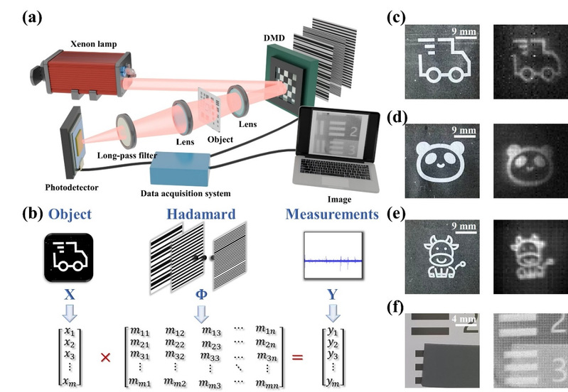
Hot-electron photodetection based on internal photoemission provides an attractive alternative to extend silicon photodetectors into the short-wave infrared (SWIR) regime.However, most reported plasmonic nanostructures rely on complex, costly, and fabrication-sensitive nanofabrication processes and exhibit inefficient hot-electron transport and extraction, which together hinder practical applications.Here, we report embedded percolated fractal metallic networks with ultrathin conformal coverage that enable efficient hot-electron transport and extraction, realized through a scalable, lithography-free, and fabrication-tolerant process based on thin-film deposition and metal-assisted chemical etching. The embedded percolated fractal metallic architecturegives rise to densely distributed plasmonic hotspotsand strong local electromagnetic field enhancement, enabling broadband hot-electron generation, while simultaneously suppressing hot-electron thermalization losses, alleviating momentum mismatch, and maximizing the emission momentum space through the formation of a quasi-omnidirectional Schottky interface. Consequently, the device achieves a responsivity of 2.78 mA/W at a wavelength of 1.3 μm, outperforming plasmonic nanoneedle arrays.Furthermore, we demonstrate SWIR single-pixel imaging with a spatial resolution of 64 × 64 pixels, including perspective imaging through silicon wafers, as well as optical communication for information transmission.This work establishes a simple, lithography-free, and fabrication-tolerant strategy for scalable, complementary metal-oxide semiconductor (CMOS)-compatible silicon sub-bandgap hot-electron photodetectors for imaging and optical communication applications.
影响因子:19
分区情况:一区
链接:https://advanced.onlinelibrary.wiley.com/doi/10.1002/adfm.75918